Plenary Lecture 4 / 5

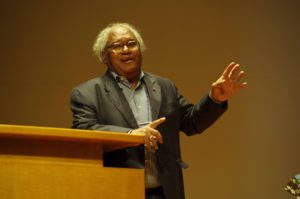
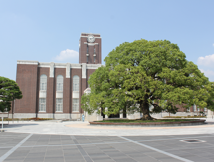
The plenary lecture 4 on carbohoration by Suzuki coupling was delivered by a novel lauriate of professor Suzuki at the Hokaito University, Japan.  And then the plenary lecture 5 on Inorganic Graphene Analogues Recent Results was delivered in the same auditorium by Professor C.N.R. Rao at the Jawaharlal Nehru Centre for Advanced Scientific Research,Bangalore, India.

These two speakers are still healthy even though over 80 years old and still have very strong energy and enthusiasm without aging effect. Professor Rao have carried out research on  materials chemistry on various functional inorganic materials. He described new 2D materials for H2 evolution as followings:  Several years ago graphene has been a sensational discovery and there are so many publications on graphene and graphene oxide. These nanosheet materials are called 2D materials. Particularly graphene is conductive materials, but not semiconductor. In the last two to three years, there has been effort to prepare graphene-like layered inorganic materials such as MoS2, WS2, GaS and BN. Several methods of synthesis of such nanosheets have been developed. Some of the recent results on few-layer transit metal chalcogenides(TMC) such as as SnSe, MoSe, WSe, and BN was presented. Specially interesting are the physical properties of these nano materials such as magnetism and superconductivity. Transistors and devices have been fabricated with many of the layered inorganic materials. A new graphene-like material is BxCyNz with high surface area and novel gas adsorptive properties. These materials have other extraordinary properties, their use as electrocatalysts being specially noteworthy. Specially noteworthy are the novel materials obtained by cross linking MoS2 with other 2D materials or by functionalizing MoS2 sheets. Thus, interaction of electron donor and acceptor molecules has unraveled the electronic structure and properties of phospherene. Covalent cross-linking C3N4 and MoS2 favors photochemical splitting of water. TIO2 was very good photocatalytic materials, however, the H2 evolution efficiency was not enough.  2D materials can be made by sonochemistry method  and chemical decomposing, and adding another functional groups by Suzuki coupling method.  This Suzuki coupling method was well introduced by the former plenary speaker.  These 2D nano materials of MoS2, SnSe, graphene and BN can be functionalzed by adding another group such as MOF (metal organic frame materials) between the mono layers of  2D materials by Suzuki coupling method.  These functionalized 2D materials showed the 10 times higher than the current developed semiconductor materials for water splitting.

After the plenary lecture, there was only one question.  It was “What is the chemical bonding between 2D materials and functional groups?  It is a covalent bonding”

Symposium A-3: Session FBS I / August 30th

Chairpersons: Akiyasu YAMAMOTO and Valeria BRACCINI 

A3-K30-001 Keynote
Vortex Pinning in iron based superconductors
Kees VAN DER BEEK

Jc and Hc2 in IBS look very interesting but way lower than in HTS (in particular in YBCO): the phase 1111 is the better performing in this respect. Flux pinning mechanisms look similar in all IBS, and have been extensively studied and presented in this talk.

Pinning centers can be nm-size inclusions, dislocations or Fe vacancies (in particular in FeSe single crystals, see very recent work by Sprau et al., 357 (2017) 65).

Jc vs field has been extensively investigated, and presents a similar behaviour in various materials. After a plateau where Jc is constant, it decreases proportionally to B^-0.5, then again it smoothest down. At low field it is predominant the contribution from big grains, isolated vortices (strong pinning on a nm scale), at intermediate fields we have collective pinning due to charged dopants / vacancies.

The depairing current density has been investigated: it presents a dome as a function of the doping, as it happens for the Tc vs x.

Vortex pinning has been correlated to the behaviour of l.

The multiple band character of superconductivity has a strong influence on Jc and on its anisotropy, which in particular in the ab direction is strongly related to the anisotropy of x.

 A3-I30-003 Invited 

Arsenic Chemistry of Iron-based Superconductors and Strategy for New Superconducting Materials
Minoru NOHARA

Prof. Nohara reported the progress of iron-based superconducting materials with the emphasis on the valence states and chemical bonds of arsenic. They demonstrated that in the novel 112-type CaFeAs2, monovalent arsenic produced As zigzag chains of CaAs intermediary layers, while trivalent arsenic produced FeAs layers. The superconducting transition temperature of this materials was enhanced up to 47 K when La and Sb were simultaneously substituted for Ca and As, respectively. Sb is preferably substituted for the As of the zigzag chains. On the other hand, in the 10-4-8-type Ca10(Pt4As8)(Fe2−xPtxAs2)5 with the highest Tc of 38 K, he emphasized that divalent arsenic produced As2 dimers in Pt4As8 layers. Finally, he discussed the structural phase transition in 122-type CaFe2As2 that is characterized by the formation of As2 dimers between the adjacent FeAs layers, which resulted in the loss of magnetism and disappearance of superconductivity. This transition can be viewed as an As2-/As3- valence transition.


A3-I30-002 Invited 

Doping dependent critical current properties in K, Co, and P-doped BaFe2As2 single crystals
Hiroshi EISAKI

Dr. Eisaki reported the in-plane critical current density (Jc) of BaFe2As2-based superconductors, Ba1-xKxFe2As2 (K-Ba122), Ba(Fe1-xCox)2As2 (Co-Ba122), and BaFe2(As1-xPx)2 (P-Ba122) in a wide range of doping concentration (x) by means of magnetization hysteresis loop (MHL) measurements on single crystal samples. Depending on the dopant elements and their concentration, Jc exhibits a variety of magnetic-field (H)- and temperature (T)- dependences. In the case of K-Ba122, the MHL of the under-doped samples (x < 0.33) exhibits the second magnetization peak (SMP), which sustains high Jc at high H and high T, exceeding 105 A/cm2 at T = 25 K and μ0H = 6 T for x = 0.30. On the other hand, the SMP is missing in the optimally- (x ~ 0.36-0.40) and overdoped (x ~ 0.50) samples, and consequently Jc rapidly decreases by more than one order of magnitude, although the change in Tc is within a few K. He pointed out that the T-dependent Jc indicates that the two pinning mechanisms, namely, the spatial variations in Tc (referred to as delta-Tc pinning) and the fluctuations in the mean free path (delta-l pinning), are enhanced for the under-doped samples, which results in the enhancement of Jc. Possible origins for the different pinning mechanism are discussed in connection with the x-dependence of Tc, the residual resistivity, AFO domain boundaries, a possible quantum critical point, etc.


A3-K30-004 Invited

Pressure Effects of FeSe by Novel DAC using metallic Diamond Electrodes
Yoshihiko TAKANO

A deep work published very recently (Matsumoto et al., JJAP 56 (2017)) has been presented, regarding the pressure effects induced in FeSe single crystals by a novel Diamond Anvil Cell.

Superconducting properties of many different materials under high pressure have recently received great attention, especially after the discovery with great surprise of superconductivity in H2S at ∼200 K under 150 GPa which was reported by resistivity measurements using a diamond anvil cell (DAC) in 2015. In fact, if one can measure the resistivity under extremely higher pressure above 300 GPa, superconductivity at room temperature in light elements such as hydrogen would be observed.

The resistivity measurement though is difficult because the sample space is very small (<100 μm) and the electrodes are deformed by compression. A novel diamond anvil cell specialized for resistivity measurements under high pressure has been developed at NIMS, Tsukuba. Once metallic diamond is heavily boron-doped, it shows metallicity and superconductivity at low temperature. Boron-doped metallic diamond electrodes were deposited onto a diamond anvil using a electron beam lithograph: in this way, resistivity measurements can be performed up to 10 GPa.

In particular, results obtained through this technique on FeSe single crystals have been reported. FeSe shows a Tc of 8 K, which can increase up to 37 K with the application of idrostatic pressure (8 GPa). When uniaxial pressure is applied, at NIMS they were able to reach Tc as high as 44 K, similarly to what happens in FeSe phase after K intercalation. This Tc increase depends on the anion height from the Fe layer which can be changed through the intercalation or through the application of the uniaxial pressure.

Oral session, A-3, August 30, 2017 (North 2F, room 28, Bulk thin films growth Microstructures I)

Chairs: Petre BADICA and Tomoya HORIDE, 13.45-15.25

4 presentations:
1 keynote (A3-K30-018 – J H Durell) – 35 min
2 invited (A3-130-019 – X Yao; A3-130-020 J Gazquez) – 25 min
1 oral (A3-O30-021- S Horii) – 15 min

Presentations introduced by P. Badica

Keynote presentation: The challenge of high filed bulk superconductors, J. H. Durell discussed the problems associated with melt textured HTS bulk superconductors especially regarding poor mechanical strength of HTS. It was emphasized the necessity to improve the mechanical properties of the materials (e.g. by metal fibers additives such as Ta) or by innovative engineering solutions using compressing metal rings to help keeping the integrity of the magnetically loaded bulk. Questions were about different possibilities of clamping and about the limitations imposed by size.

Invited presentation 1: The artificial control of film microstructures in LPE-processes YBCO by tuning solute supersaturation state, X. Yao introduced different aspects of the crystal growth of REBa2Cu3O7 superconductors (especially by liquid phase epitaxy method). The possibilities to control growth and quality of materials were discussed (e.g. by using non-stroichiometric compositions, or the appropriate conditions of cooling based on thermodynamic aspects of the supersaturation). Questions were about film thickness and spiral growth mechanism.

Attendance: good – about 20 persons

Schedule: according to the program

Atmosphere: relaxed, friendly, collaborative

Symposium C-5: Frontier of Nano-Materials Based on Advanced Plasma Technologies

A Challenge for Future Carbon Devices by Advanced Plasma Nano-Processes

Masaru Hori of Nagoya University, Japan, gave a fantastic keynote lecture in the oral session of Symposium C-5 in the morning session on August 30. He has investigated advanced plasmas as a synthesis method, the growth mechanism, control of structure, and applications for nano-carbons. First, he presented fabrication of the tough fuel cell devices with carbon nanowalls (CNWs), where Pt nanoparticles were supported on CNWs by super critical CVD after the growth of CNWs. Second, he explained that the triple phase plasma employing the ethanol alcohol showed the high speed and high quality nano graphene synthesis for a high performance of fuel cell device. Then, he concluded that nano carbons, especially CNWs, had a great potential as a key material for future industrial and medical applications.

Fabrication of High-Mobility Amorphous In2O3:Sn Films by RF Magnetron Sputtering with Impurity-Mediated Amorphization Method

Naho Itagaki of Kyushu University, Japan, gave an excellent keynote lecture in the oral session of Symposium C-5 in the afternoon session on August 30. She proposed an impurity mediated amorphization (IMA) method, where the impurity was introduced to the conventional control parameters (temperature and pressure) for crystal growth. She explained that high mobility (> 50 cm2/Vs) and nanocrystal-free a-ITO films have been obtained, and the a-ITO films were grown even at higher temperature than the crystallization temperature (150°C) of In2O3. In addition, the a-ITO films fabricated via IMA showed high thermal stability, which means that the amorphous structure was maintained even after they were annealed at 300°C.


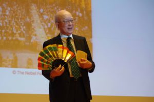
Keynote lecture scene by Prof. Hori.

Keynote lecture scene by Prof. Itagaki.

Sômiya Award ceremony and presentation

This IUMRS-SOMIYA Award is named in honor of Professor Shigeyuki Sômiya. IUMRS manages this award program for encouragement of active international collaboration in materials science field. In this time, five active teams applied to this selection.

Past two award winners examined all application forms on the basis of following three criteria.

The team to be honored must have collaborated across at least two continents some time during the last decade.

The collaborative work must be of the highest quality and well recognized by the international materials community.

The impact on technology or society is also a major factor.

The award commission chair Professor Robert Chang officially approved examination reports.

Then IUMRS-SOMIYA Award 2017 goes to following collaborative work and team.

Award winning work;

Semiconductor Nanowires: Growth, Characterization, Processing and Optoelectronic Devices

Team leader: Professor Chennupati Jagadish (Australian National University, Australia)

Members:
Professor Leigh M. Smith (University of Cincinnati, USA)
Professor Michael B. Johnston (Oxford University, UK)
Professor Jin Zou (University of Queensland, Australia)
Professor Antonio Polimeni (University of Rome La Sapienza, Italy)

On 30
th August from 5 pm, the award ceremony was organized at Yoshida Campus.

Photographs are beautiful smile of winners and award presenter.

Left: award presenter Professor Jim Williams
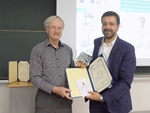
Right: Team leader Professor Chennupati Jagadish


Left: award presenter Professor Jim Williams
Right: Team member Professor Antonio Polimeni